Building the ALU - Nand2Tetris Unit 02
The journey is continuing. This unit we are building the ALU. The ALU is a part of a computers CPU, which usually does logical and arithmetic operations on binary numbers.
The ALU we are building is rather simple.
- HalfAdder - Adding two bits with sum and a carry
- FullAdder - Handling the carry
- Add16 - Add two 16 bit registers
- Inc16 - Increment a 16 bit register by 1
- ALU - Combining all of the above in a Chip
My implementation of the ALU Chip in HDL
CHIP ALU {
    IN
        x[16], y[16],  // 16-bit inputs
        zx, // zero the x input?
        nx, // negate the x input?
        zy, // zero the y input?
        ny, // negate the y input?
        f,  // compute (out = x + y) or (out = x & y)?
        no; // negate the out output?
    OUT
        out[16], // 16-bit output
        zr,      // if (out == 0) equals 1, else 0
        ng;      // if (out < 0)  equals 1, else 0

    PARTS:
    // zx
    Mux16(a=x, b[0..15]=false , sel=zx, out=zeroedX);
    // nz
    Not16(in=zeroedX, out=notX);
    Mux16(a=zeroedX,b=notX,sel=nx, out=processedX);
    //zy
    Mux16(a=y, b[0..15]=false , sel=zy, out=zeroedY);
    //ny
    Not16(in=zeroedY, out=notY);
    Mux16(a=zeroedY,b=notY,sel=ny, out=processedY);
    // f
    And16(a=processedX , b=processedY , out=andXY);
    Add16(a=processedX , b=processedY , out=addXY);
    Mux16(a=andXY, b=addXY,sel=f, out= fOut );
    // no
    Not16(in=fOut, out=notF);
    Mux16(a=fOut, b=notF, sel=no,
    // variable wire
    out[0..7]=finalResultp1,
    out[8..15]=finalResultp2,
    // out
    out=out,
    out[15]=ng
    );
    //zr
    Or8Way(in=finalResultp1 , out=zr8wayoutp1);
    Or8Way(in=finalResultp2 , out=zr8wayoutp2);
    Or(a=zr8wayoutp1, b= zr8wayoutp2, out=zrOut);
    Not(in= zrOut, out= zr);
    //ng
    // output from Mux16 in no
}
Key Insight
The ALU is a pipeline. Just like many other things in computing. If statements is not a thing and you must expect the current to go through everything. You can’t route it. This you have to take into account when you build it. Managing the 0 and 1 state and handling the data either way. Early returns is not possible.
What Surprised Me
How elegant and simple hardware design is designed. All the block build on each other and many things are reused. That’s an elegance that I appreciate.
My Struggle
Thinking like a programmer and not a hardware coder. Everything runs in parallel. Also had to understand the control bits.
- zx, nx, zy, ny, f, no. Made no sense to me in the beginning. Implementing slowly and reading the material a couple of times helped me.
The hardest part was for sure implementing the ALU. Also struggled with using existing chips to create the new ones. HDL syntax is a little bit challenging but I’m learning it slowly and their online editor is good.
Creating a diagram of the FullAdder before writing the code
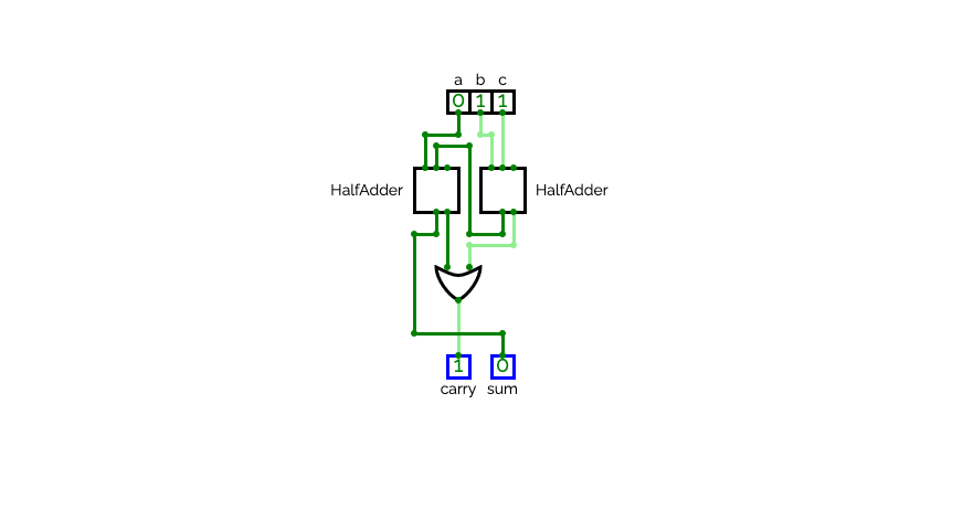
Drawing out the FullAdder logic helped me visualize how the carry bit flows through the circuit. The diagram shows how two HalfAdders combine with an OR gate to handle the previous carry input, making the addition of three bits possible.
The Connection
I like how there is a real connection between the Unit 01 and this 02. It’s getting more clear. All the Chips build on top of each other.
- HalfAdder -> FullAdder -> Add16
- Inc16 uses the Add16
- ALU is eveything
And I know from course research that the ALU will be the computational center of the CPU which we will be build later.
Plan Now
Unit 03. The sequential logic. Storage, state, time. Looking forward to it.
See you around!